Digital simulation
The purpose of digital simulation is to determine the nodal values of a network of which the elements are characterized by a discrete system. Each digital element reads the digital signal on its input, performs some Boolean logic operation, optionally saves the state, and places a calculated signal on its output after a specified delay.
Logic levels
A logic level is a specific voltage or a state in which a digital signal can exist. In a digital circuit, a signal has three possible states: HIGH (1), LOW (0), or Undefined. The strength of a signal is typically described by its voltage level.
For the Digital components and the Digital probe, you can configure the logic levels, such as the standard or threshold voltage levels, in the Item tab of the configuration pane. You can also configure the design-wide logic levels in the Document tab and apply the settings to all objects in the design by checking the Use document settings option for each component in the Item tab.
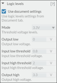
The following options are available in the Logic levels section:
Note The output voltage options are not applicable to Digital probe. The input voltage threshold options are not applicable to Digital Constant and Digital Clock.
- Mode—Standard to use for the threshold voltage levels. The threshold voltage values are predefined and read-only unless you select Custom.
- Output high—Minimum output voltage level to produce a HIGH signal.
- Input high threshold—Minimum input voltage level for the signal to be considered HIGH.
- Output low—Maximum output voltage level to produce a LOW signal.
- Input low threshold—Maximum input voltage level for the signal to be considered LOW.
For example, if you select the 3.3V mode, an input signal with a voltage level of 0.8V or smaller than 0.8V is considered LOW. An input signal with a voltage level of 2V or greater than 2V is considered HIGH. Input signals with voltage levels between 0.8V and 2V are considered invalid. Similarly, an output signal with a voltage level of 0V is considered LOW. An output signal with a voltage level of 3.3V or greater than 3.3V is considered HIGH. Output signals with voltage levels between 0V and 3.3V are considered invalid.
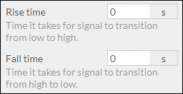
Rise time and fall time
One consideration for digital simulation is the rise time and fall time, which are the time it takes for the signal to transition from low to high or vice versa in physical circuits.
Each digital device has a rise time and fall time associated with it. In most cases, the time is short enough to be ignored. However, as you connect more devices to a digital circuit, the rise time and fall time adds up to a sizable delay time which may create operational problems in high-speed digital circuits, such as flip-flops, where state changes may occur very fast.
To ensure that a digital simulation reflects the actual behavior of the physical circuit, NI recommends that you specify the rise time and fall time of the digital components in the Item tab of the configuration pane.